The G8TMV Keyer Project

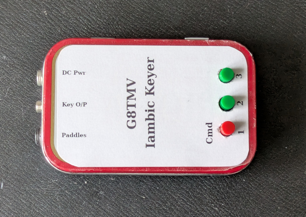
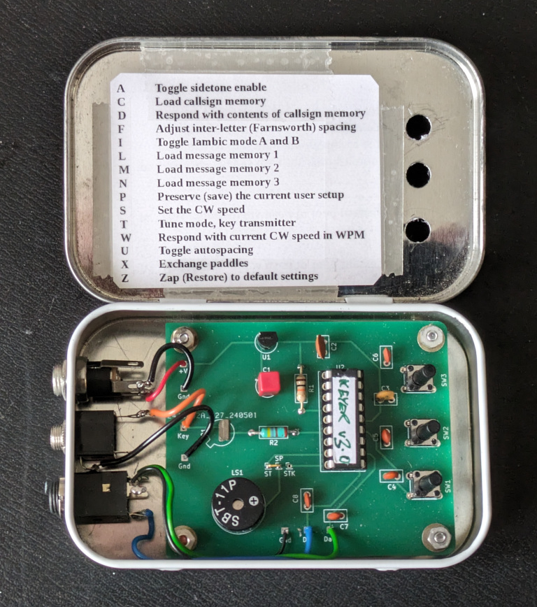
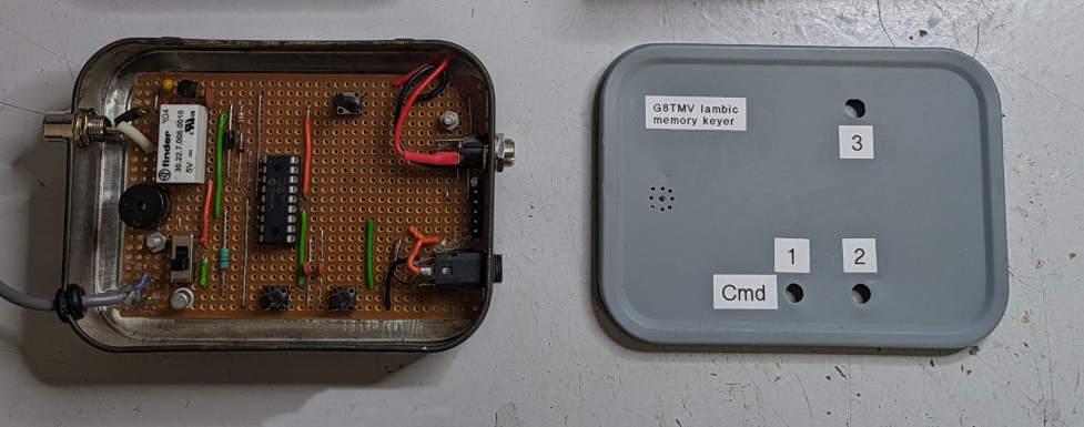
The CW keyer is designed to fit into a traditional Altoids tin. The basic design started as a clone of an old K1EL shareware keyer intended to be used with my FT-817. The first prototype got hi-jacked to drive an old WW2 transmitter (see below).

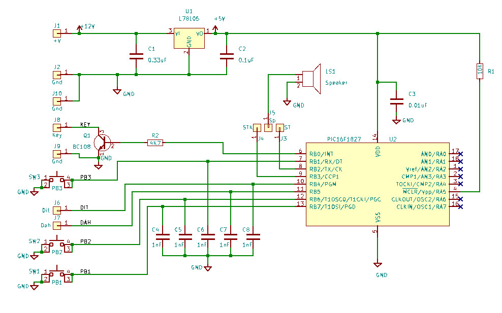
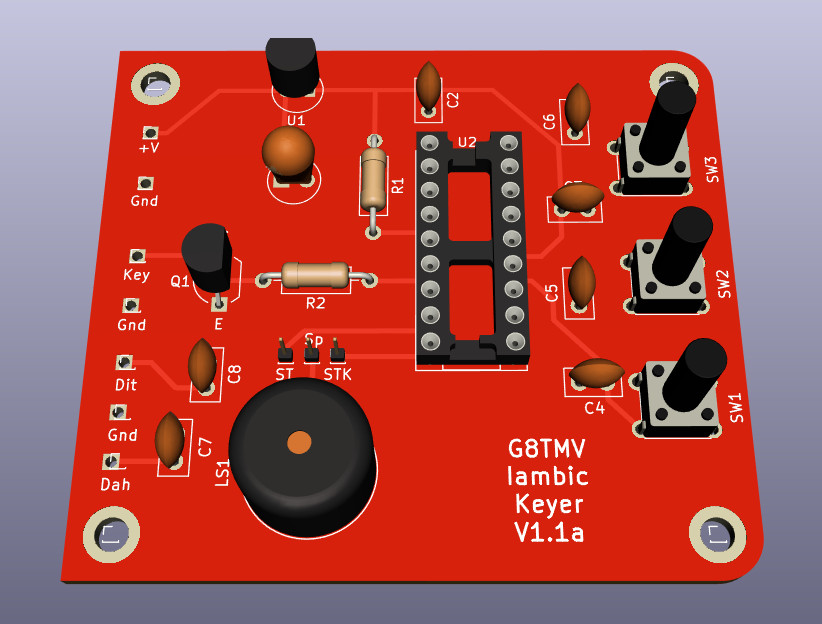
I've made several enhancements and upgrades to the hardware and software to improve usability and functionality including implementing 3 user loadable non-volatile memories and a separate callsign memory which can be inserted into any of the stored messages so that the user only needs to change the callsign once to update all of it's uses.

Full details are available in the operating manual available here.

The CW Keyer Pre-production build. CW keyer early production version


An internal view of the CW Keyer Pre-production build. CW keyer early production version

The pre-production version was built into an Altoids tin using one of the pre-production PCBs. The full production PCBs (see image below) have been shortened to allow more room for the connectors and the layout has been changed slightly to ease the wiring.

The CW Keyer circuit diagram. CW keyer circuit

A BoM is available here. The links in the Speaker circuit allow the builder to use either a buzzer or a passive speaker. Transistor Q1 can be any general purpose NPN device, it needs to handle the keying voltage from the Transmitter. The keyer uses approx 4mA while idle, 6mA key-down with the sidetone off and 18mA key-down with the sidetone on. The system runs entirely from the on-board 5v regulator, supply voltages should be between 7v and 12v depending on the regulator fitted.

A 3D view of the CW Keyer V1.1 Design.
3D view

The CW Keyer prototype. CW keyer Prototype

The prototype was originally developed for use on a WW2 Wireless Set 12 and so has relay keying as a switchable option to cope with the -60 volt keying line. The 3rd button was a later addition to the design, which explains the odd placement.


Valid HTML 4.01! Valid CSS!